If you want to "see" physical objects whose dimensions are measured in nanometers and simultaneously probe the electronic structure of the atoms, molecules, and surfaces populating this nanoworld, you just might have to invent a new microscope. In fact, that's exactly what Fellow David Nesbitt's group recently accomplished.
Oliver Monti, a former JILA postdoc currently at the University of Arizona, graduate student Tom Baker, and Nesbitt have invented a microscope capable of analyzing the make-up and properties of nanoscale electronics and nanoparticles.
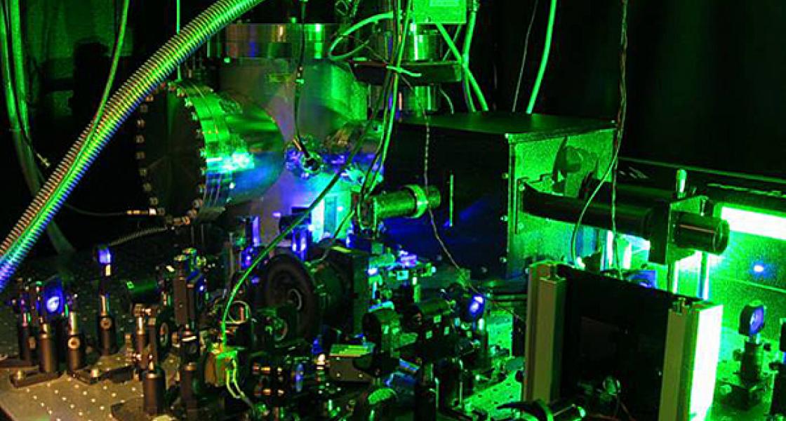
The group's new scanning photoionization microscope (SPIM) is shown above. It includes an optical microscope in a vacuum chamber and an ultrafast laser, which appears blue in the foreground. It combines the high spatial resolution of optical microscopy with the ability to detect low-energy electrons emitted by a material illuminated with laser pulses.
The ability to monitor photoelectron emission should make it possible for the microscope to detect electronic patterns in devices such as nano-scale transistors or electrode sensors and to identify their chemical constituents. At the same time, the new microscope can make a physical picture of the tiny structures.
"You make images by virtue of how readily electrons are photoejected from a material," Nesbitt explains. "The method is in its infancy, but nevertheless it really does have the power to provide a new set of eyes for looking at nanostructured metals and semiconductors."
The Nesbitt group recently confirmed the accuracy of its new technique in comparisons of SPIM images of nanostructured gold films with scans made using atomic force microscopy. They also determined that SPIM images can detect spikes in electron energy, or current, with sufficient resolution to detect variations in material thickness and estimate the depth of electrons escaping from a metal sample. The group is currently working on enhancing SPIM to make chemically specific images. - Julie Phillips